
At a Glance
- Neurophos claims its photonic AI chip will run at 56 GHz, delivering 235 Peta Operations per Second while consuming 675 watts.
- The startup raised $110 million in Series A funding led by Gates Frontier.
- The chip is said to outperform Nvidia’s B200 GPU in both speed and energy efficiency.
Neurophos, a photonics startup spun out of Duke University, says its new optical chip could outpace Nvidia’s GPUs in speed and power efficiency. The company has raised $110 million in a Series A round led by Gates Frontier, with Microsoft’s M12 and other investors. The announcement comes as AI labs look for ways to scale compute while curbing energy use.
David R. Smith, a Duke professor, first demonstrated a metamaterial cloak that could hide objects from a single microwave wavelength two decades ago. Although the cloak was limited in scope, the research opened new avenues in manipulating light and heat. Smith’s work laid the groundwork for the photonic technologies Neurophos now pursues.
Neurophos was founded by Smith’s former students and is backed by the Metacept incubator, also run by Smith. The company’s mission is to solve the biggest bottleneck for AI labs: scaling compute power without a proportional rise in power consumption. It focuses on optical processing units that can perform matrix-vector multiplication faster than silicon-based GPUs.
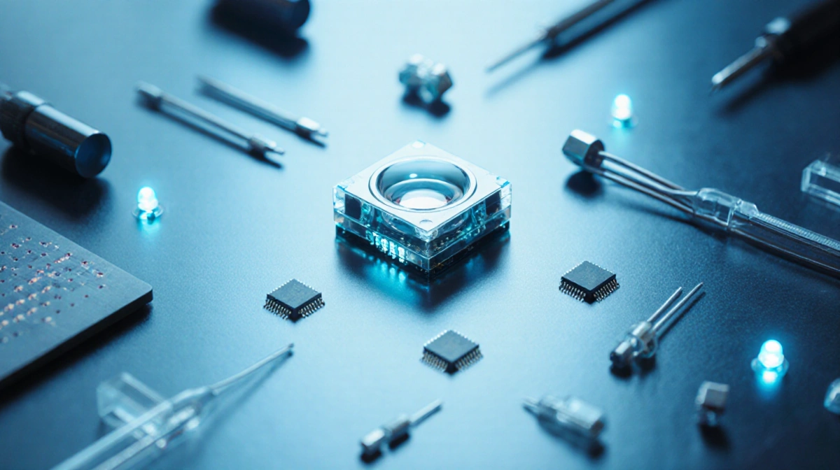
The startup’s core innovation is a metasurface modulator that functions as a tensor core processor. By arranging thousands of these modulators on a single chip, Neurophos claims the device can perform many calculations in the optics domain before converting data back to electronics. This approach, according to the founders, eliminates the energy cost of frequent data conversion.
Neurophos says its metasurface modulator is 10,000 times smaller than conventional optical transistors. The reduced size allows the company to pack more units onto a chip, increasing parallelism and throughput. The team argues that the smaller footprint also lowers heat generation and power draw.
The startup’s chip can run at 56 GHz, a speed that is far beyond what current silicon GPUs can achieve. At this frequency, the device delivers a peak of 235 Peta Operations per Second. In contrast, Nvidia’s B200 GPU can deliver only 9 POPS while consuming 1,000 W.
“If you shrink the optical transistor, you can do way more math in the optics domain before you have to do that conversion back to the electronics domain,” said Dr. Patrick Bowen, CEO and co-founder, told News Of Philadelphia. He added that solving energy efficiency first is essential to achieving higher speeds.
Bowen also noted that the performance gap is not just incremental. “What everyone else is doing is evolutionary, tied to TSMC’s node improvements, which average 15% energy efficiency gains every few years,” he said. “By the time we launch in 2028, we will still have massive advantages over Nvidia.”
According to Bowen, the company’s metasurface modulators will provide a 50× edge over Nvidia’s Blackwell architecture in both raw speed and energy efficiency. He emphasized that the chip’s 675 W power draw is lower than the B200’s 1,000 W while delivering more than 20 times the computational throughput.
The Series A round closed with $110 million in funding. Gates Frontier led the investment, joined by Microsoft’s M12, Carbon Direct, Aramco Ventures, Bosch Ventures, Tectonic Ventures, Space Capital, and others.
Neurophos is positioning itself against Nvidia, the most valuable public company that has dominated the AI hardware market. Other photonic firms, such as Lighmatter, have shifted focus to interconnects rather than compute. The startup’s unique approach could carve out a niche in high-performance inference.
The company has already signed multiple customers, though it declined to name them. Microsoft is reportedly “looking very closely” at the startup’s technology, according to a statement from the company. The interest from major players underscores the potential impact of Neurophos’s chips.
Bowen expressed confidence that the performance and efficiency gains will act as a moat. He compared the company’s progress to Nvidia’s evolutionary path, noting that TSMC’s nodes only improve energy efficiency by about 15% over several years. By 2028, the startup aims to outpace Nvidia by a wide margin.
Neurophos faces a crowded market where silicon GPUs have been the standard for AI inference. Nvidia’s GPUs have underpinned the AI boom, but the company’s optics-based design could shift the balance. The startup’s claim of a 50× advantage in speed and efficiency is a bold assertion.
Other photonic companies have struggled to scale due to the large size of optical components and the need for data converters. Neurophos claims its metasurface solves these problems by being 10,000 times smaller than traditional optical transistors. This reduction in size is key to the chip’s high density and low power consumption.
Neurophos also plans to use standard silicon foundry materials, tools, and processes to manufacture its chips. By leveraging existing silicon infrastructure, the company hopes to reduce fabrication complexity and cost. This approach could make the technology more accessible to data-center operators.
The startup expects its first chips to hit the market by mid-2028. The timeline is based on the current development cycle and the availability of silicon foundry capacity. The company will begin with integrated photonic compute systems for data-center use.
Neurophos will produce datacenter-ready OPU modules that include a full software stack and early-access developer hardware. The modules are designed to integrate with existing GPU-based workflows. The company believes this strategy will ease adoption by AI labs.

Neurophos is also opening a new engineering site in San Francisco while expanding its headquarters in Austin, Texas. The expansion supports the company’s growing engineering and sales teams. The move reflects the startup’s ambition to become a major player in AI hardware.
The fresh capital will fund the development of the integrated photonic compute system. It will also support the creation of OPU modules and the accompanying software stack. Early-access hardware will allow developers to test the technology in real workloads.
Neurophos intends to use part of the funding to open the San Francisco engineering site. The site will focus on hardware design, testing, and system integration. It will also house a small but highly skilled team of photonics experts.
Additional investment will go toward expanding the Austin headquarters, where the company’s core engineering and business functions reside. The expansion will accommodate new hires and support the growing customer base. The company sees this as a critical step toward mass production.
Neurophos has already signed contracts with several unnamed customers. The company also reports that Microsoft is closely evaluating the technology. These partnerships signal early market validation for the startup’s photonic approach.
Dr. Marc Tremblay, corporate vice president and technical fellow of core AI infrastructure at Microsoft, said in a statement that “modern AI inference demands monumental amounts of power and compute.” He added that a breakthrough like Neurophos’s could meet those demands.
Key Takeaways
- Neurophos’s optical chip could outperform Nvidia’s B200 GPU in both speed and energy efficiency.
- The company raised $110 million in Series A funding led by Gates Frontier.
- The startup’s metasurface modulators are 10,000 times smaller than traditional optical transistors, enabling high density.
- The first chips are expected by mid-2028, built with standard silicon foundry processes.
If Neurophos delivers on its promises, it could reshape how AI inference is performed in data centers.